
AD University Of Sargodha (UOS) 2025
Discussion
Ask a question about this paper, or help someone else with theirs. Answers are emailed to whoever asked.
No questions yet — be the first to ask.
Paper text
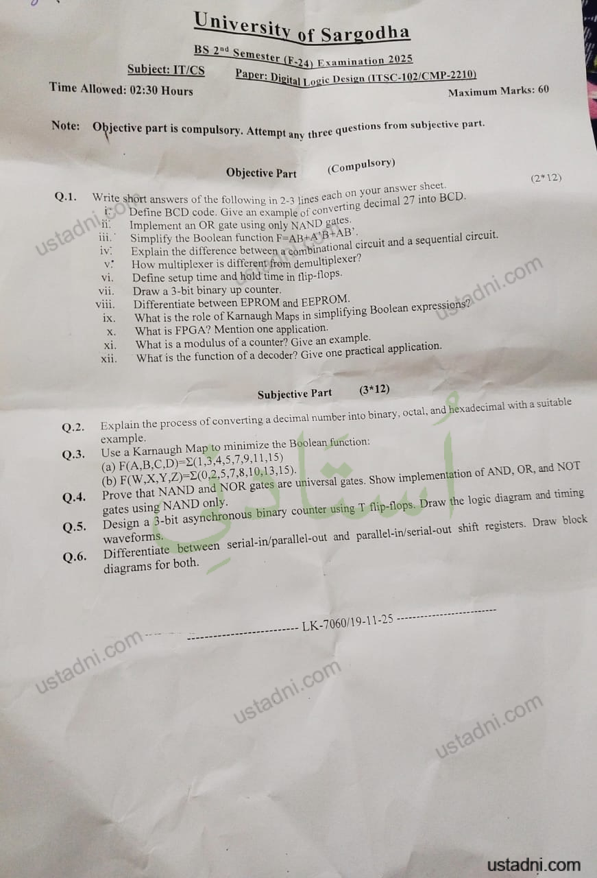
Univers;
S
2 ly of Sargodha
2nd em
Subject: IT/CS “Ser F. 4) Examination 2025
Time All Paper; igita] | ogic Design (ITSC-1 2/CMP-2210
ERE 0230 Hours Maximum Marks: 60 A
Note: Objective part is compulsory, Attempt apy three questions from subjective part.
Objective Part (Compre)
(2*12)
fed ny answer sheet
Q.1. W nte short answers of the following in 2-3 ines each ony i 27 into BCD.
17+ Define BCD code. Give an example of converting .
IL. Implement an OR gate using only NAND BCS
Hi." Simplify the Boolean function F=AR+A'B*AD ial circuit.
es - : equential ©
Iv. Explain the difference between a combinational pita Spe
v: How multiplexer is different from demultiplexer
vi, Define setup time and hold time in flip-flops
vil. Draw a 3-bit binary up counter. 4
viii. Differentiate between EPROM and EEPROM. . Ni
: ces pl Xpressions:
ix. What is the role of Karnaugh Maps in simplifying Boolean exp
X. What is FPGA? Mention one application.
xi. What is a modulus of a counter? Give an example. a
: : n.
xii. What is the function of a decoder? Give one practical applicatio
& “a
|
Subjective Part (3*12)
2.
Maximum Marks: 60
Objective Partis compulsory, 5 :
+ Attempy any three questions from subjective part.
Objective Par (Compulsory)
Write sh
1. :
i: Do ae hi following in 2.3 Jines each on your answer sheet (2*12)
ii aid > : D code. Give an example of converting decimal 27 into BCD.
Hie ement an OR gate using only NAND gates.
des FPL the Boolean function F=Ap+A'B+AB’.
vi Hoo ihe difference between a gombinational circuit and a sequential circuit.
Vie. Den mu tiplexer is different from demultiplexer?
1 B ine Setup time and hold time jj flip-flops. _
viii’ Draw a 3-bit binary up counter
3)
: gL reatiaie between EPROM and EEPROM
X. What + i or OL nang Maps in simplifying Boolean expressions?
: ; 5 10n one application.
J hat isa modulus ofa CONE an example.
. at is the function of a decoder? Give one practical application.
— _— A «i £* on A oh
Subjective Part (3*12) TR :
Explai > sesOf convert: :
Rn process of converting a decimal number into binary, octal, and hexadecimal with a suitable
Use a Karnaugh Map to minimize the Boole
an function:
(a) F(A,B,C,D)=2(1,3,4,5,7.9,11,15) Hi
(b) F(W,X,Y,Z2)=%(0,2,5,7,8,10,13,15).
Prove that NAND and NOR gates are universal gates. Show implementation of AND, OR, and NOT
gates using NAND only.
Design a 3-bit asynchronous binary counter using T flip-flops. Draw the logic diagram and timing
waveforms.
Differentiate between serial-in/parallel-out and parallel-in/serial-out shift registers. Draw block
diagrams for both.
LK-7060/19-11-25 -seseeseareecarmmresees