
Digital logic Design BSIT University Of Sargodha (UOS) 2020
Discussion
Ask a question about this paper, or help someone else with theirs. Answers are emailed to whoever asked.
No questions yet — be the first to ask.
More Digital logic Design papers
See all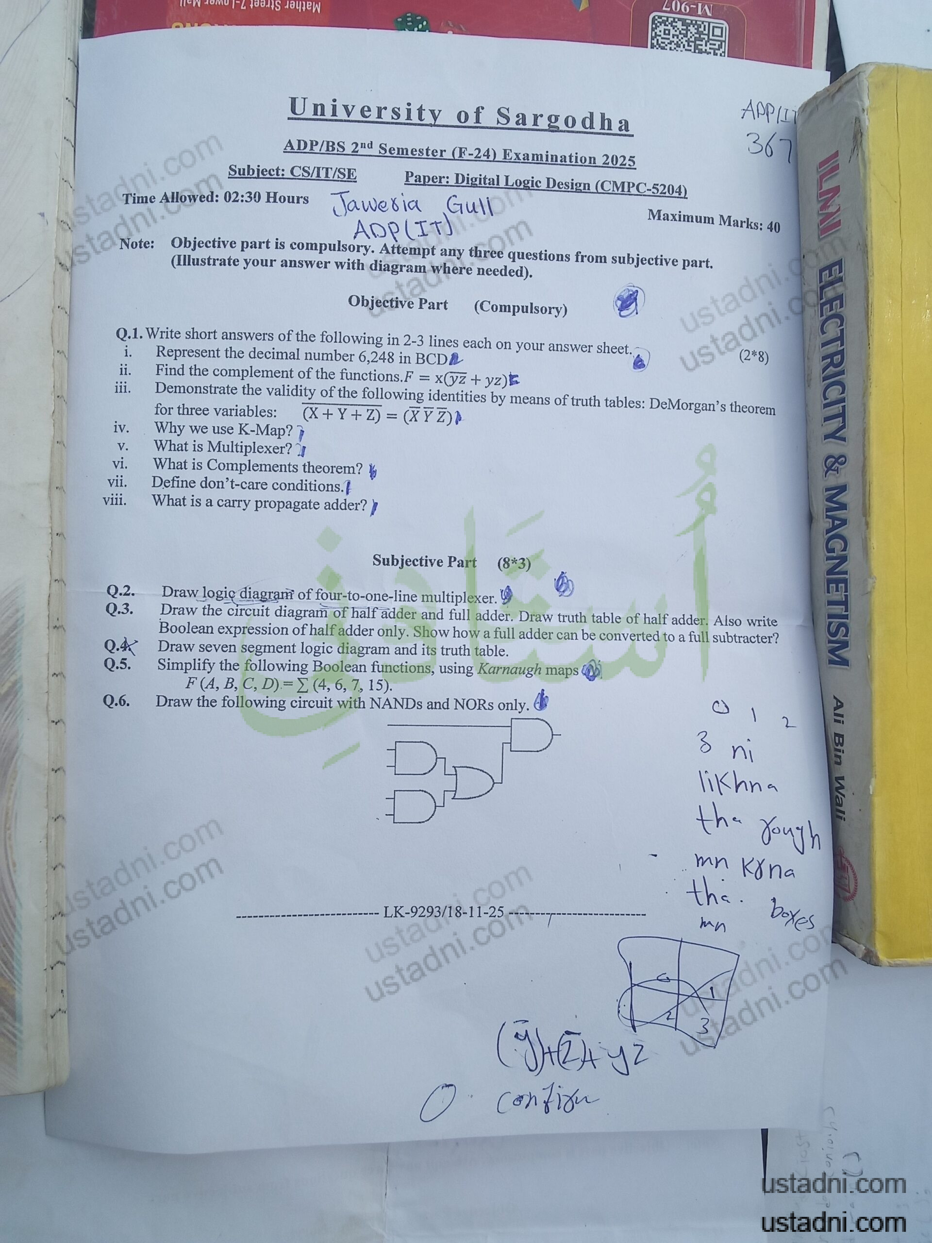 Digital logic Design ADP/BS 2 Semester/Term University Of Sargodha (UOS) 2025
Uploaded 1 month ago · by Jaweria Gull
Download ↓
Digital logic Design ADP/BS 2 Semester/Term University Of Sargodha (UOS) 2025
Uploaded 1 month ago · by Jaweria Gull
Download ↓
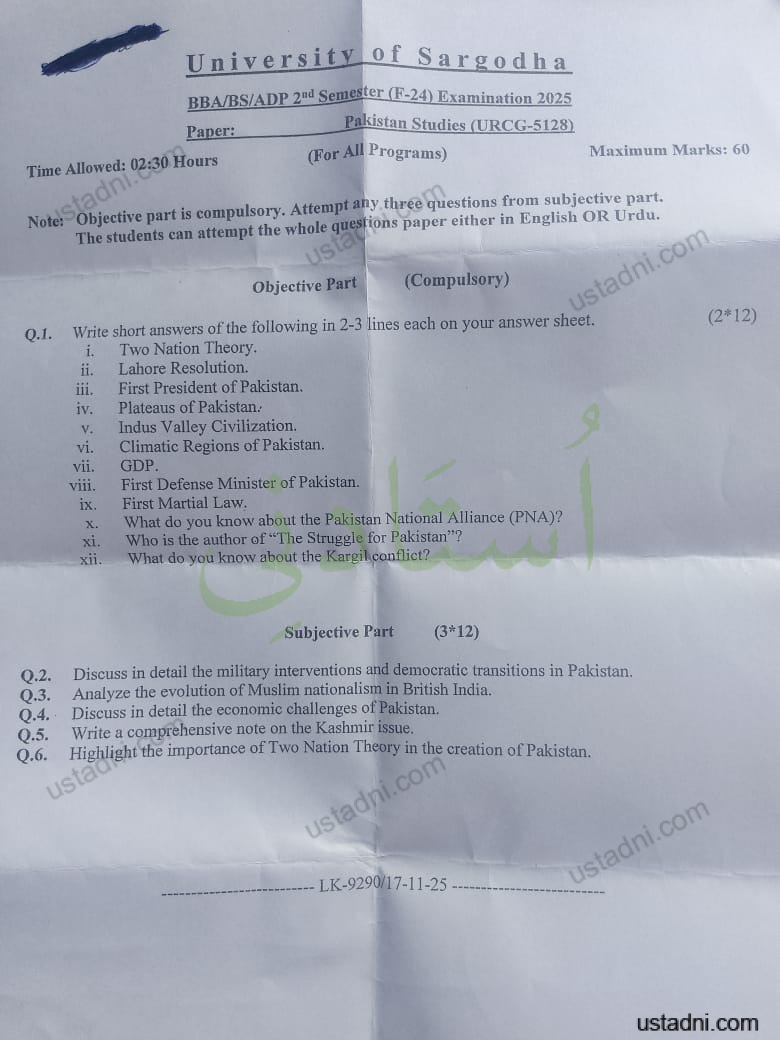 Digital logic Design ADP/BS University Of Sargodha (UOS) 2025
Uploaded 2 months ago
Download ↓
Digital logic Design ADP/BS University Of Sargodha (UOS) 2025
Uploaded 2 months ago
Download ↓
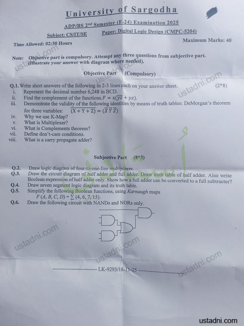 Digital logic Design ADP/BS University Of Sargodha (UOS) 2025
Uploaded 2 months ago
Download ↓
Digital logic Design ADP/BS University Of Sargodha (UOS) 2025
Uploaded 2 months ago
Download ↓
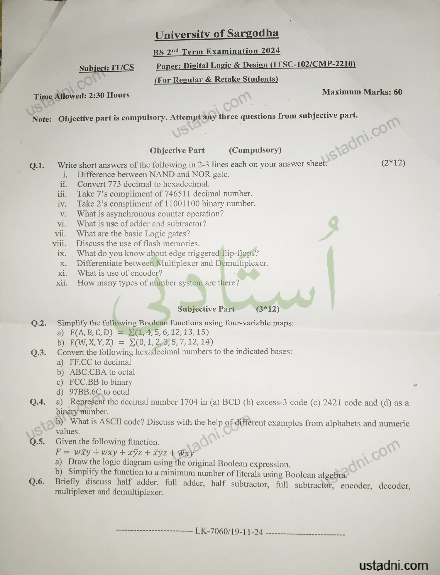 Digital logic Design BS 2 Semester/Term University Of Sargodha (UOS) 2024
Uploaded 11 months ago
Download ↓
Digital logic Design BS 2 Semester/Term University Of Sargodha (UOS) 2024
Uploaded 11 months ago
Download ↓
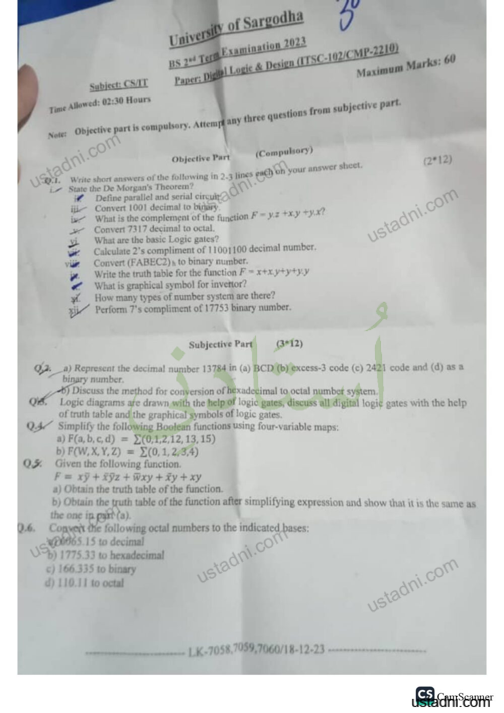 Digital logic Design BS University Of Sargodha (UOS) 2023
Uploaded 1 year ago
Download ↓
Digital logic Design BS University Of Sargodha (UOS) 2023
Uploaded 1 year ago
Download ↓
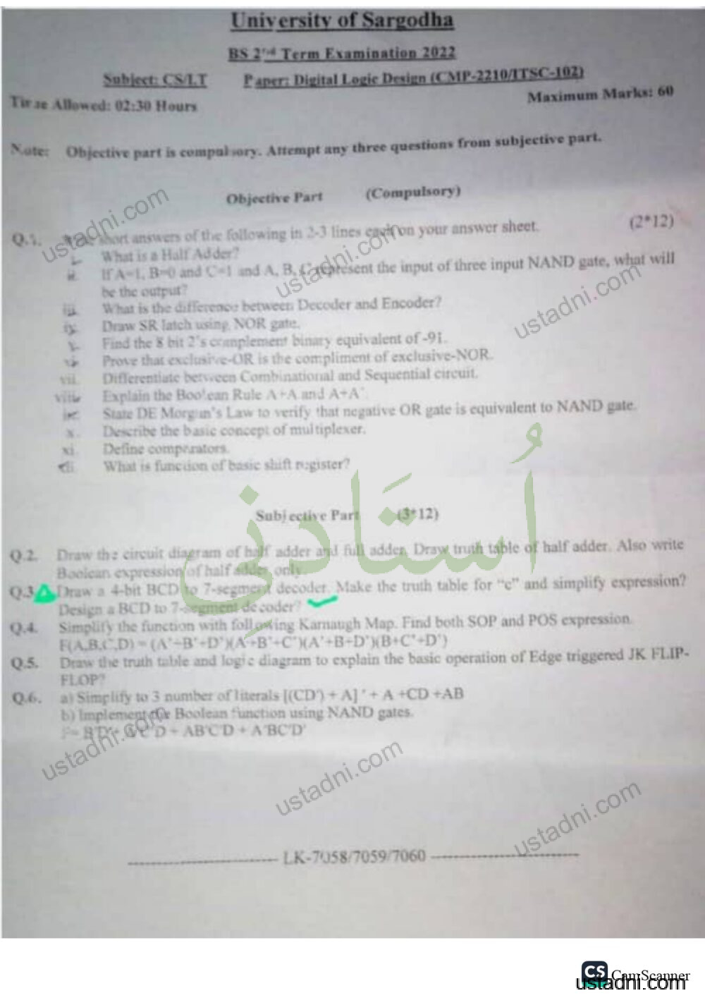 Digital logic Design BS University Of Sargodha (UOS) 2022
Uploaded 1 year ago
Download ↓
Digital logic Design BS University Of Sargodha (UOS) 2022
Uploaded 1 year ago
Download ↓
Paper text
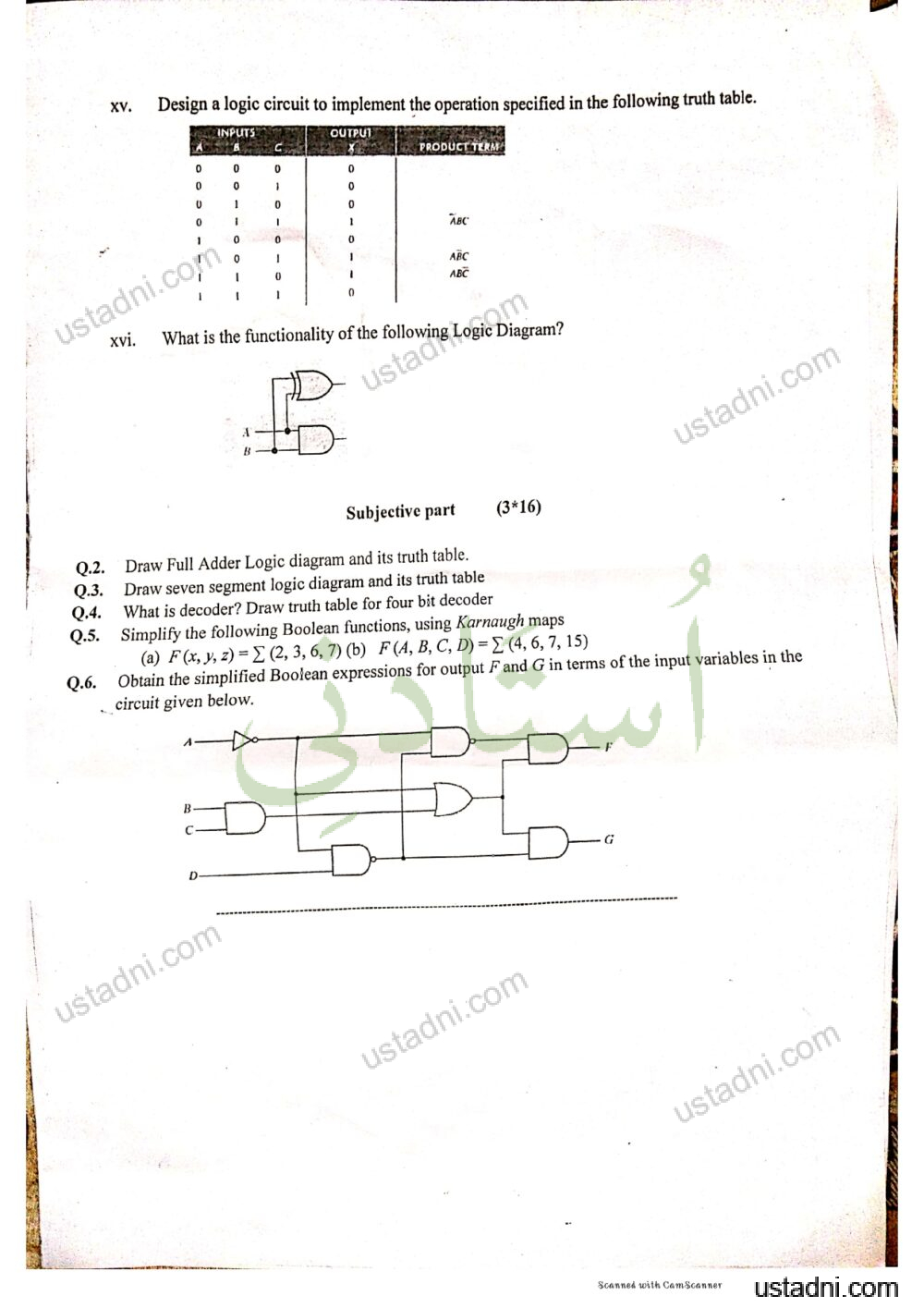
XV.
Design a logic circuit to implement the operation specified in the following truth table.
INPUTS
OUTPUT
PRODUCETE
0
ABC
ABC
ABC
ustadni.ce
XVi.
What is the functionality of the following Logic Diagram?
usto
ustadni.com
Q.2.
Q.3.
Q.4.
Q.5.
Q.6.
Subjective part
(3*16)
Draw Full Adder Logic diagram and its truth table.
Draw seven segment logic diagram and its truth table
What is decoder? Draw truth table for four bit decoder
Simplify the following Boolean functions, using Karnaugh maps
(a) F(x, y, z) = 2 (2, 3, 6,
7)
(b) F (4, B, C,
D) = 2 (4, 6, 7,
15)
Obtain the simplified Boolean expressions for output F and G in terms of the input variables in the
circuit given below.
1-
• G
ustadni.com
ustadni.com
ustadni.com
Scanned with CamScanner
ustadni.com